Showing posts with label nanoart. Show all posts

Sunday, January 16, 2011

MRS Fall 2010 Science as Art Competition

Every year, in the spring and fall of the northern hemisphere, scientists from around the world congregate, like moths to a flame, for a lovein of sharing, learning and networking. Known as the Materials Research Society meetings, these biannual events have become a must attend for those in search of unbridled materials knowledge.

Beyond knowledge however, there is beauty and since 2006, this group of burly scientists have been devoting their time to the more aesthetically pleasing forms of their science. An event of science meets art, which has simply become known as the MRS Science as Art Competition.

These are the winners of the Material Research Societies, 2010 Fall, Science as Art Competition.

1st Place Winner | The silk collective | Konstantinos Tsioris, Tufts University

Thursday, August 19, 2010

IBM Demonstrate New Nano Patterning Tool

Nanotechnology is perhaps THE cutting edge technology of the 21st century. However, production of nano particles of all types remain fairly expensive compared to more conventional ways of using the same materials.

However thanks to IBM researchers, the status quo could be about to change for the technique of nano patterning.

IBM scientists have developed a new technique that uses a nano scale tip, that when forced to a surface and heated sufficiently is able to carve away substrate material from the surface to create 2D and 3D patterns and structures as small as 15 nanometres at greatly reduced cost and complexity.

Click on the images bellow for a thorough explanation and access to higher resolution pictures.

Image courtesy of Advanced Materials

Monday, August 16, 2010

Art and the Atom

I came across a news release recently, via Google news and discovered that in Christchurch, New Zealand, there is an interesting exhibition merging nanotechnology and art.

The exhibition is a collaboration between the University of Canterbury and the MacDiarmid Institute for Advanced Material and Nanotechnology that aims to bring scientists and artists together in order to communicate a brilliant 21st century technology to the public.

Nanotechnology is the engineering of materials the size of 1 billionth of a meter. When materials are built at such a small scale and of variant sizes, different properties, that which don't appear in it's chemical makeup at macro sizes spring forward, often surprising the scientists at work: Nano silver is completely anti-bacterial, carbon nano tubes are execellent conductors of electricity.

The MacDiarmid Institute donated $2000 dollars to be awarded to the best nanotechnology picture of the exhibition.

David Garret | Towers of Vertically Aligned Nano Tubes

Friday, July 30, 2010

MRS "Science as Art" Competition(s)

After uncovering the following photos, I decided that my first two blogs could be considered a practice... because the ensuring pictures blow the others out of the water!

These first two pictures of science imitating art are my favourites from the series. We are able to see these pictures due to the magic of the Scanning Electron Microscope (SEM). The "Field of Sunflowers" were produced by S.K. Hark, Chinese University of Hong Kong and won 1st prise in the 2008 sprint meet. The Second image was produced by Wen Hsun Tu, National Taiwan University, Taipei, Taiwan and titled "Nano-Witch" was the 2nd Place Winner in the 2009 fall meeting.
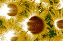
2008 Spring Meet - 1st Place Winner - Field of Sunflowers - S.K. Hark, Chinese University of Hong KongBoth images are composed of what is known as nanowires. Each nanowire is about 10 nm in diameter and tens of micrometers in length. They were grown from a silicon oxide (SiOx) compound for the sunflowers and a zink oxide (ZnO) for the nano-witch. Both use a process known as Vapour-Liquid-Solid (VLS) to grow the nanowires.

Thursday, July 29, 2010

Art of Science Gallary 2010

On the second day of SaCrIt i blogged some neat photos...

The following photos are held a Princeton University webserver. They appear to have run some sort of competition for the best science related photos and have done so for 2010, 2009, 2006 & 2005. Don't ask me what happened to the other years.

Here are the three winners. Click on the images to read about how they were created. Much of the details bellow are in deed paraphrased as i understand very little of it.

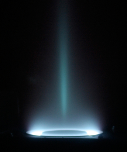
This Xenon Plasma Accelerator uses electronic and magnetic fields to accelerate xenon propellant to produce thrust. Xenon is a colourless gas but we can see a blue haze here due to the result of the xenon being excited by electric discharge - like the blue zap of static electric shock we're all too familiar with, although this is a form of electrostatic discharge, but you get the idea. Plasma Accelerators are a leading technology for future space flight... and it looks darn pretty too.

Credits:Jerry Ross (fac) - PPPL


Wednesday, July 28, 2010

Art On A Chip

In my daily reading of newscienist.com I came across their exposé of a flickr photo stream detailing parts of circuit designs and other related images that have an underlying beauty/symmetry. In fact, my hunger to share these images is what sowed the seed for creation of this blog.

Here are the photos New Scientist found most striking. Click on each image to see what New Scientist had to say about how these marvellous works were created.

Image: Chris Sip and Albert Folch/University of Washington(Image: Chris Sip and Albert Folch/University of Washington)


copyrighted